


Chips, also known as integrated circuits (ICs), are the core components of modern electronic devices. They integrate billions of electronic components, such as transistors, resistors, and capacitors, through complex circuit structures to achieve specific functions. The internal structure of a chip is highly complex, involving multiple levels and components, ranging from microscopic transistor-level structures to macroscopic system-level designs.
Basic Components
1. Transistors
Types: The fundamental building blocks of chips are transistors, mainly MOSFETs (Metal-Oxide-Semiconductor Field-Effect Transistors), including NMOS and PMOS types.
Structure: A transistor consists of a source, drain, and gate, with the gate positioned above an insulating layer between the source and drain.
Working Principle: It operates based on electric fields that control the carriers in the channel, enabling switching and current amplification.
2. Metal Layers (Interconnects)
Used to connect transistors and other electronic components, forming complex circuit networks.
Made of copper or other metals, insulated by dielectric layers.
The width and spacing of the interconnects determine the chip's integration level and performance.
Functional Modules
Chips contain multiple functional modules that work together to achieve specific functionalities. Below are some common functional modules:
1. Logic Gates
Comprise basic logic gates (AND, OR, NOT, etc.) and more complex logic functional units.
Serve as the foundation of computer processors and other logic circuits.
2. Arithmetic Logic Unit (ALU)
Responsible for performing basic arithmetic and logic operations within the CPU.
3. Cache Memory
High-speed storage units of different levels are used to temporarily store frequently accessed data, accelerating data exchange between the processor and main memory.
Internal Structure of Specialized Chips (Example: FPGA)
FPGA (Field-Programmable Gate Array) chips feature a highly configurable internal structure. Their main components include:
1. Programmable Logic Units
The fundamental building blocks of FPGAs contain lookup tables (LUTs), flip-flops, and other logic units.
It can be configured by users to form various combinational or sequential logic circuits.
2. Internal Interconnects
Include programmable interconnect lines and switch matrices to link different CLBs (Configurable Logic Blocks) and form desired logic functions.
3. Input/Output Units
Interfaces for FPGA interaction with external circuits, supporting multiple electrical standards and offering programmability.
4. Embedded Functional Modules
Such as embedded multipliers, high-speed serial communication interfaces, DSP modules, and high-performance processors.
These hardwired modules are predefined during manufacturing, offering better performance and lower power consumption.
5. Clock Management Modules
Handle clock generation, distribution, and management within the FPGA, including components like PLL (Phase-Locked Loop) and DLL (Delay-Locked Loop).
6. Embedded Storage Resources
Used to build cache, FIFO (First-In-First-Out) buffers, lookup tables, and other data storage structures.
Other Key Components
1. Packaging
After fabrication, chips undergo packaging to isolate them from external environments while enabling connections via pins to external circuits.
Packaging may include multi-layer substrates and auxiliary circuits.
2. Power Management and Thermal Design
Ensures chip stability and reliability during operation, including power distribution networks, power estimation and management units, and necessary thermal management solutions.
Advanced Technologies and Structures
As technology advances, chip design and manufacturing continue to evolve. Below are some cutting-edge technologies and structures:
1. FinFET (Fin Field-Effect Transistor)
To address short-channel effects, transistors are designed with a fin-like structure, enhancing electric field control over the channel.
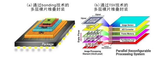
2. 3D Stacking Technology
Examples include 3D NAND flash memory and three-dimensional integrated circuits, which improve storage capacity and integration density by stacking chip layers vertically.
3. SoC (System-on-Chip)
Integrates multiple functional modules into a single chip, forming a complete system.
SoC technology significantly enhances system integration and performance.
The internal circuit structure of a chip is a highly integrated and complex system, encompassing fundamental transistors, interconnect layers, advanced functional modules, and cutting-edge technologies. With continuous technological progress, chip design and manufacturing will evolve towards higher performance, lower power consumption, and smaller sizes.