


Since the invention of the first transistor by three scientists from AT&T Bell Laboratories, Bardeen, Brydon, and Shockley, in 1947, they simultaneously created the history of microelectronics packaging. In order to facilitate the use and welding of transistors in circuits, there must be external pins on the housing; in order to fix the small semiconductor chip, there must be a housing base to support it; in order to protect the chip from atmospheric pollution and to make it strong and durable, it is There must be a case to seal the chip, etc. With the rapid development of China's semiconductor industry, the market size of semiconductor packaging materials is also expanding. According to relevant data, China has become one of the world's largest markets for semiconductor packaging materials, and market demand continues to grow.
Ⅰ. Packaging function
Packages usually have five functions, namely power distribution, signal distribution, heat dissipation channels, mechanical support and environmental protection.
1. Power distribution
Microelectronic packaging must first be able to connect to the power supply so that current can flow between the chip and the circuit. Secondly, different parts of the microelectronic package require different power supplies. It is necessary to properly distribute the power supply to different parts to reduce unnecessary power loss. This is particularly important on multi-layer wiring substrates. At the same time, the distribution of ground wires must also be considered.
2. Signal distribution
In order to minimize the electrical signal delay, the interconnection path between the signal line and the chip and the path leading out through the I/O of the package should be as short as possible during wiring. For high-frequency signals, crosstalk between signals should also be considered for reasonable signal distribution wiring and ground wire distribution.
3. Heat dissipation channel
Various microelectronic packages must consider how to dissipate accumulated heat when devices and components operate for a long time. Different packaging structures and materials have different heat dissipation effects. For microelectronic packages with high power consumption, additional heat sinks or forced air cooling or water cooling should also be considered to ensure that the system can work normally within the range of operating temperature requirements.
4. Mechanical support
Microelectronic packaging can provide strong and reliable mechanical support for chips and other components, and can adapt to changes in various working environments and conditions.
5. Environmental protection
Many parameters of semiconductor devices and circuits, such as breakdown voltage, reverse current, current amplification coefficient, noise, etc., as well as the stability and reliability of the device are directly related to the state of the semiconductor surface. Many process measures in the manufacturing process of semiconductor devices and circuits are also targeted at semiconductor surface problems. After semiconductor chips are manufactured, they are always under threat from the surrounding environment until they are packaged. During use, some environmental conditions are extremely harsh, and the chip must be tightly sealed and encapsulated.
Ⅱ. Packaging processIt is important to understand the entire packaging process steps so that the package can be designed, manufactured and optimized. In many cases, packaging (Assembly) and silicon wafer manufacturing (IC Fabrication) are not completed in the same factory. Although there is a tendency to integrate the front-end process and the packaging process into the same production line, in most cases the silicon wafer still needs to be transported to the packaging factory.
Chips are usually tested on-chip on the silicon wafer process line, and defective chips are marked, usually with a black ink dot or laser mark, to prepare for the subsequent packaging process. When chip mounting The automatic pick-up machine can automatically distinguish qualified chips from unqualified chips.
The packaging process can generally be divided into two parts: the process step before encapsulating it with plastic packaging material is called Assembly or Front End Operation, and the process step after molding is called Back End Operation. End Operation). In the previous process, the purification level is controlled between 10 and 1,00. In some production companies, the molding process is also carried out in a purification-controlled environment. However, it is difficult to achieve a purified environment above Class 10,000 due to dust in the mechanical hydraulic press and preforms used in transfer molding operations. Generally speaking, though, as silicon chips become more complex and miniaturized, more assembly and molding processes will take place in dust-controlled environments.
Most of the packaging materials used today are polymers, so-called plastic packaging. There are also many types of molding technologies for plastic packaging, including transfer molding, injection molding, and pre-molding. Among them, transfer molding technology is the most commonly used.
The typical process of transfer molding technology is as follows: Place the frame tape with the chip mounted and chip interconnection completed in the mold, preheat the plastic packaging material (between 90-95 (o)C), and then put it into the transfer molding into the transfer tank of the machine. Under the pressure of the transfer molding piston, the plastic compound is extruded into the sprue and injected into the mold cavity through the gate (170-175 (o)C). The plastic sealing material solidifies quickly in the mold. After a period of pressure holding, the module reaches a certain hardness. Then the module is ejected with an ejector pin and placed in a curing furnace for further solidification.
To sum up, it requires multiple processes such as silicon wafer thinning, silicon wafer cutting, chip mounting, chip interconnection, molding, deburring, rib cutting, bending, soldering, and coding.
Ⅲ. Moore Elite Packaging Services
The semiconductor packaging materials industry has high technical requirements and requires continuous technological research and development and innovation. In this regard, Moore Elite has strong technical strength and R&D capabilities, and can continuously launch new products and new technologies.
Moore Elite Packaging and Testing has successfully delivered 4780+ quick seals & 105+ SiPs, increasing test efficiency by more than 50%. The packaging service mainly focuses on the three major businesses of engineering batch fast sealing, system-level SiP packaging design, and packaging mass production management. It has deployed 20,000-square-meter packaging and testing factories in Hefei, Wuxi, and Chongqing, with an investment of more than 400 million yuan in core equipment.
Wuxi factory production capacity: packaging: SiP 100 million pieces/year, FC 36KK/year, QFN 420 million pieces/year;
Chongqing factory production capacity: 500 batches for quick sealing in one month;
Hefei factory production capacity: 300 batches can be quickly sealed in one month.
Moore Elite Packaging and Testing Collaborative Solution
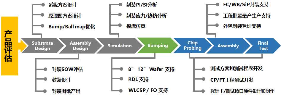
System-in-Package SiP
Moore Elite SiP one-stop solution runs through the product life cycle from circuit design to packaging and mass production, allowing customers to maximize worry and effort. Customers only need to input product functional requirements, such as existing PCB schematics, and subsequent design and production can be completely completed by Moore, who will coordinate and complete schematic design, chip selection, component selection, SiP design, production and testing. At present, Moore Elite has served a number of leading system manufacturers including TCL, CRRC, and Changhong, as well as small and medium-sized solution/module manufacturers targeting diversified markets.

Flip-chip flip-chip packaging
Moore Elite Wuxi SiP Advanced Packaging and Testing Center provides complete Flip-Chip packaging solutions for DPU, HPC, CPU, GPU, high-end servers, high-performance ASSP, FPGA and other products, including packaging design, simulation, engineering batch and mass production. The overall production capacity of SiP/FCCSP/FCBGA can reach 5KK per month.